Home Capabilities
PCB MANUFACTURING CAPABILITIES
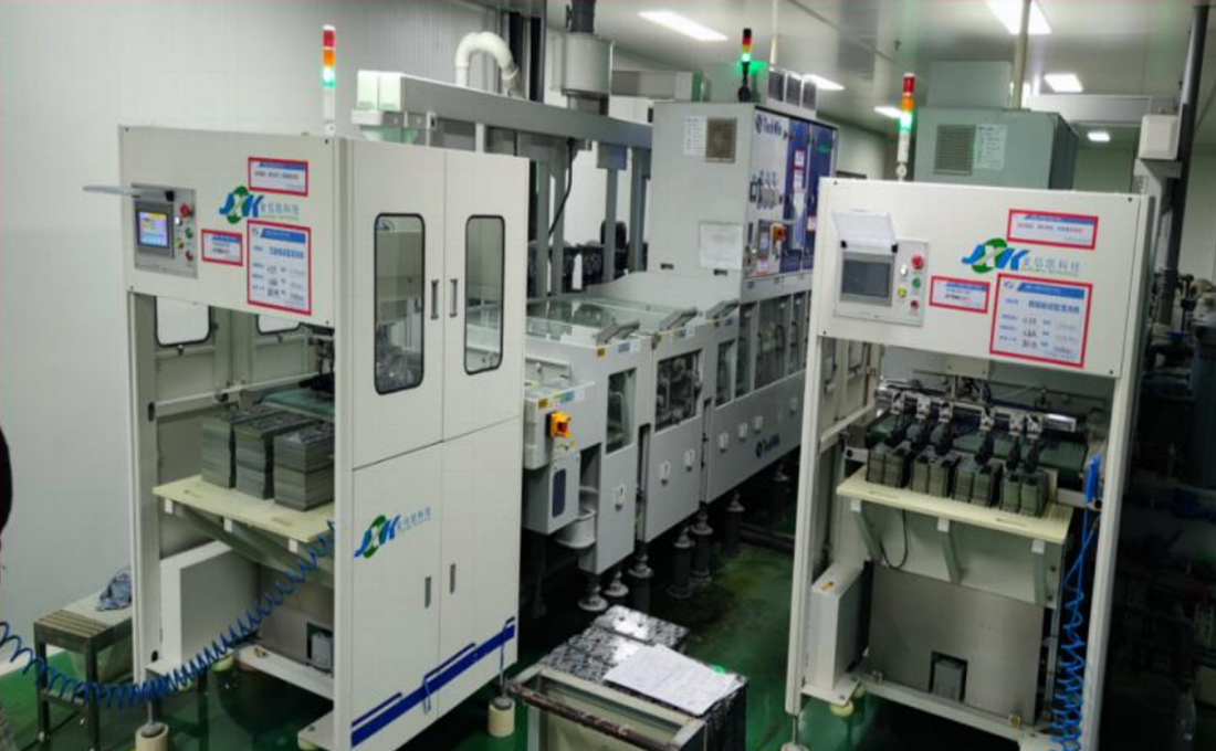
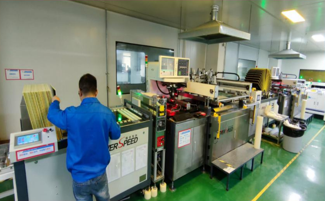
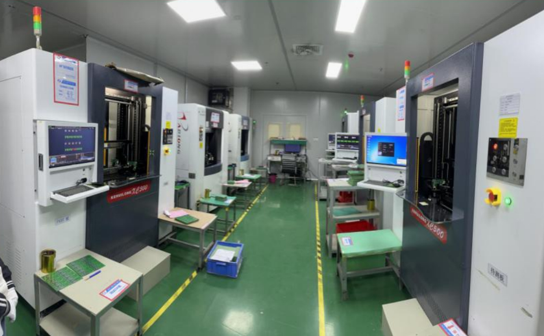
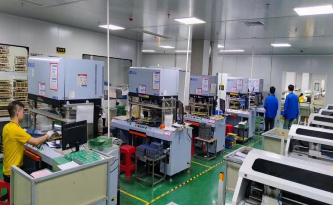
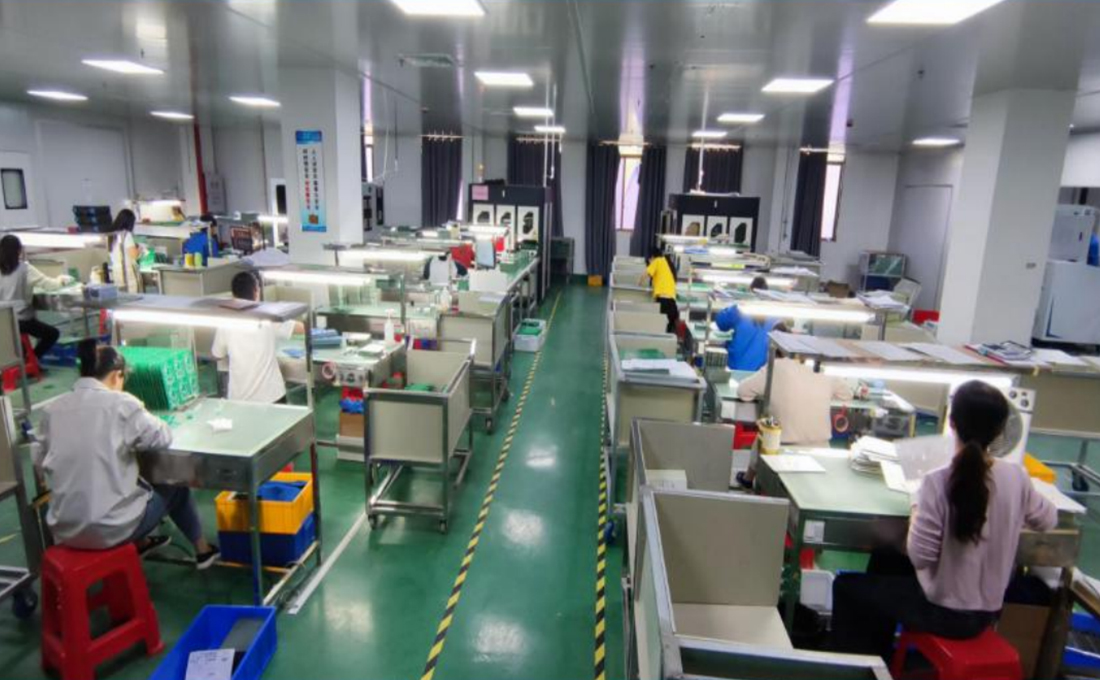
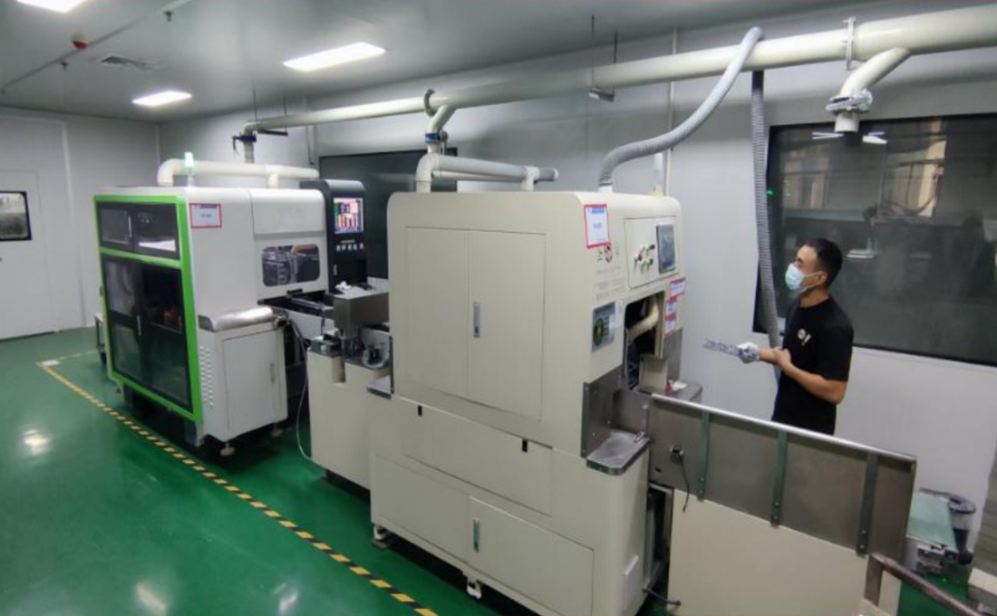
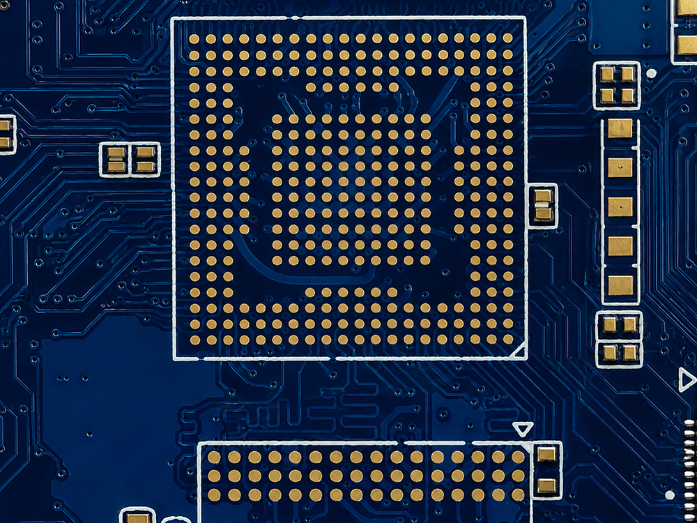
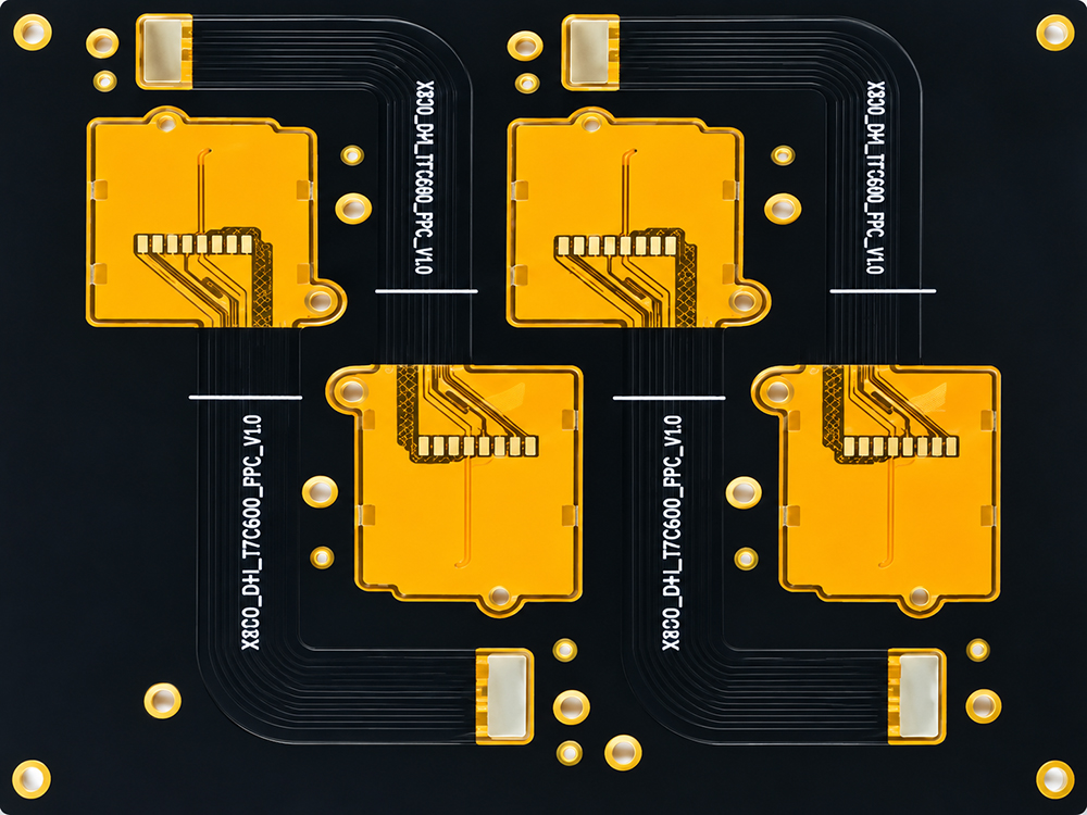
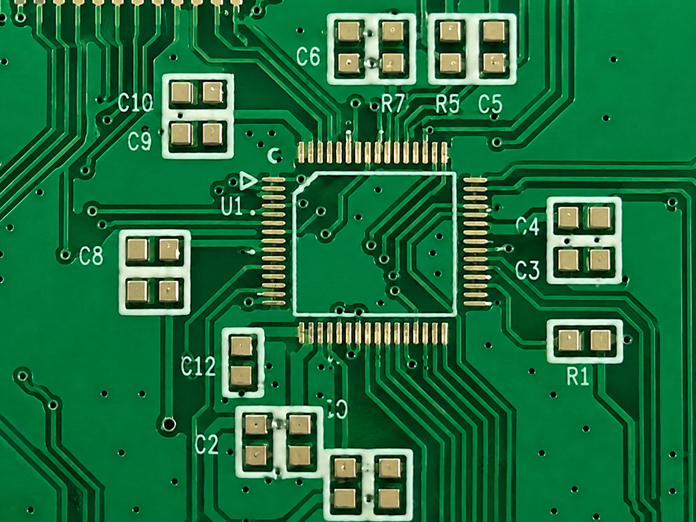
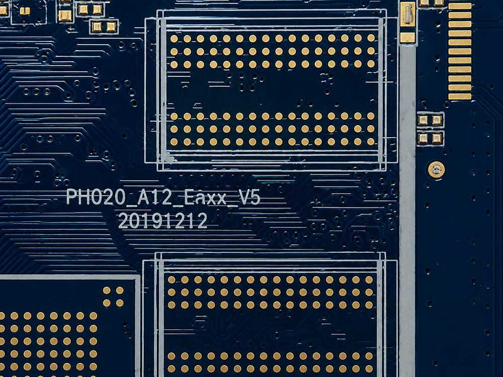
Advanced manufacturing equipment, strict process control andexperienced team ensure high quality PCBs for your products.

Flexible layer count

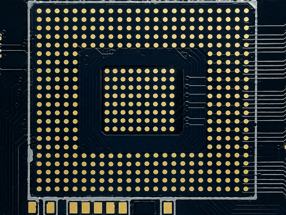
Fine line and small hole

Strict QC system

Quick turnacound

DFM & technical support

Best value for you
Capabilities Overview
Detailed Specifications
| BASIC CAPABILITIES | MATERIALS | SURFACE FINISH | |||
|---|---|---|---|---|---|
| Layer Count: | 1 – 20 Layers | FR-4 (Tg 130/150/170) | HASL (Lead Free) | ||
| Board Thickness: | 0.2 – 6.0 mm | HI-Tg FR-4 | ENIG (Electroless Nickel Immersion Gold) | ||
| Finished Copper Thickness: | 0.5 – 8.0 oz | Aluminum Base | OSP (Organic Solderability Preservative) | ||
| Min. Line / Space: | 3 / 3 mil | Copper Base | Immersion Silver | ||
| Min. Line Width (Inner Layer): | 2.5 mil | Rogers (RO4003C, RO4350B, RO4450F, etc.) | Immersion Tin | ||
| Min. Line Width (Outer Layer): | 3 mil | Taconic | Hard Gold | ||
| Min. Hole Size (Drilled): | 0.15 mm (6 mil) | PTFE (Teflon) | ENEPIG | ||
| Min. Hole Size (Laser): | 0.10 mm (4 mil) | Polyimide (PI) | Other (upon request) | ||
| Aspect Ratio: | Up to 10 : 1 | High Frequency Materials | |||
| Max. Panel Size: | 600 × 1200 mm | Other Special Materials | |||
| Max. Board Size: | 500 × 600 mm | ||||
| Board Shape: | Rectangle, Round, Irregular | COPPER WEIGHT | SOLDER MASK | ||
| V-cut: | ±0.1 mm | Inner Layer Copper: | 0.5 – 6.0 oz | Color: | Green, Blue, Black, White, Red, Yellow |
| Routing Tolerance: | ±0.1 mm | Outer Layer Copper: | 0.5 – 8.0 oz | Type: | LPI / Dry Film |
| PTH Tolerance: | ±0.075 mm | Heavy Copper: | Up to 12 oz | Min. Solder Mask Dam: | 0.05 mm |
| NPTH Tolerance: | ±0.05 mm | Min. Solder Mask Opening: | 0.05 mm |
| Special Processes | ||
|---|---|---|
| Blind / Buried Via | Controlled Impedance | Via in Pad |
| HDI PCB (Microvia) | Differential Impedance | Press-fit Hole |
| Stacked Via | Embedded Copper | Resin Plugged / Filled Via |
| Back Drilling | Sequential Lamination | Carbon Ink / Silver Paste |